I have plans for a small weather station that’s been lying on my hard drive for a while. The basic design includes ESP8266 modules that send data over to a Raspberry Pi base station that logs all that data and can create graphs. I’ve done a good deal of prototyping and breadboarding for the electronics, so the last step left was to create a PCB and package it so I could use it for real.
Since I don’t have the material to etch my own PCB with chemicals and copper plates at home, and that I want something that looked professional, I’m looking at having my board created by a fabrication house. I will also need to create many boards at once since I want to support having many modules to capture the temperature in various locations.
Fortunately, creating your own board is pretty cheap nowadays. You’ll need to learn how to draw your board in a EDA (Electronics Design Automation) software, but it’s not that hard if you’ve already done the electronics. For this project, I used KiCad, which is open source and works on Windows, Linux and Mac. The free version of Eagle is another popular option for DIY electronics, but since KiCad has improved a lot in the last few years I choose to test it.
If you want to check the KiCad files for the project, it’s available on my GitHub at https://github.com/CindyPotvin/TemperatureLogger_ESP-12F.
Circuit Schematic
You always need to start with a schematic to define the logic between your different parts using symbols before moving to the PCB design. The software will then help you respect that logic while you are designing the PCB. In KiCad, the design is done in the Eeschema module.
At this point, you just drop all your part on a sheet and wire them up. All the parts you should need for a simple project should already be included with KiCad, but you always have the option to create your own. Also, most places where you’ll purchase your parts such as Digikey and Mouser also offer symbols and footprints for KiCad and other popular EDA software.
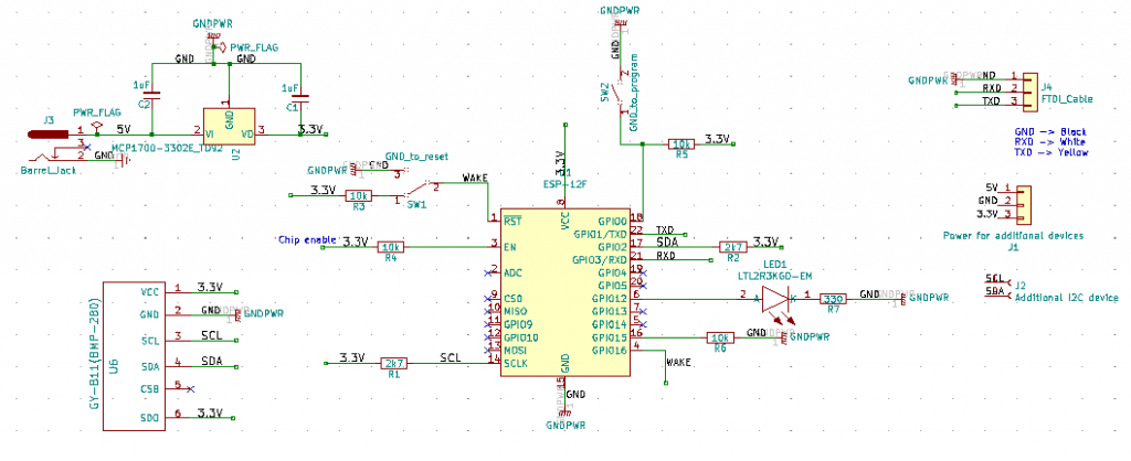
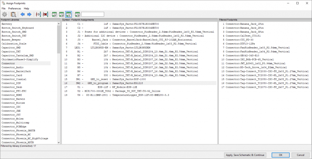
Eeschema also includes an Electrical Rules Check tool that validates if all the part were wired up correctly. Once the schematic is ready, you’ll need to associate the schematic symbols to the footprints, which represent the real components that will be on the board. In Eeschema, this is the Assign Footprints option:
Parts that you downloaded often already have footprints, but you’ll need to choose one for basic parts such as headers, resistors and capacitors since they can have various sizes, orientations and packages.
The last step is to run the Generate Netlist tool in Eeschema to export all the logical rules and the associations you just created so you can use them during the PCB design process.
PCB Design
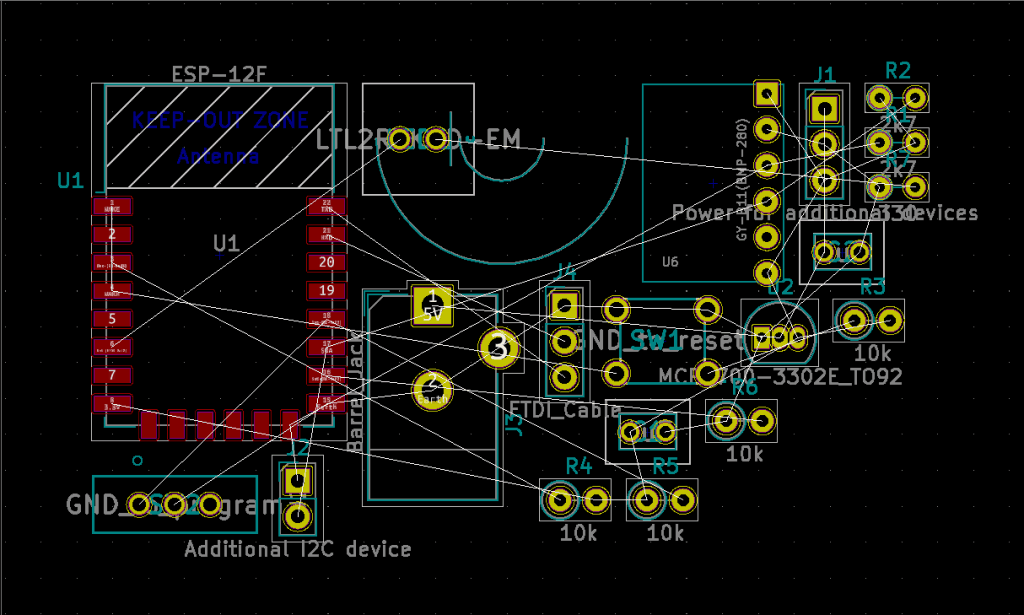
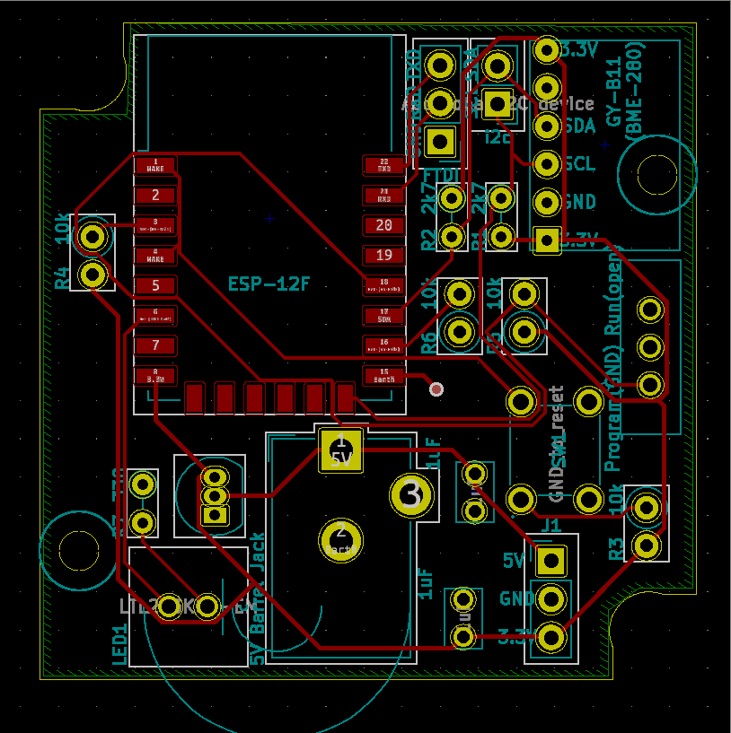
In KiCad, the PCB design module is called Pcbnew. To get started, you need to import the Netlist you just created from your schematic in a blank sheet. When it’s done importing, it will dump all the components in a pile on the board so you can place them. It also includes thin lines representing all the connections you’ll need to complete the board.
Defining the board size
Before you start wiring up components, it’s best to define the edge of the board and try to place the components in it. PCB are priced by the area and the number of layers, so you’ll want to limit the size of the board, especially if you want to produce many copies. You may also have a specific enclosure you wish to fit the circuit in; it’s certainly easier to make the PCB the right size than finding the perfect box afterwards.
You only need to draw the edge on the proper layer (Edge.cuts) using the graphic lines in KiCad and when they’ll fabricate the board they’ll know where to cut. It can also include cutouts and holes if you need to mount the circuit somewhere. You can then drag and drop the components inside, rotate them and try to see if everything fits. The 3D Viewer can be a great help here, even if not all the parts have a 3D representation.
Board setup
The basic setup from KiCad is already good enough for most projects, but it’s worth checking out with your PCB fabrication house what are their constraints so you do things that supported. For this project, I ordered with Elecrow (more on my choice in the Ordering the PCB section), so here are their basic constraints at the time I’m writing this:
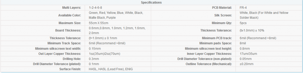
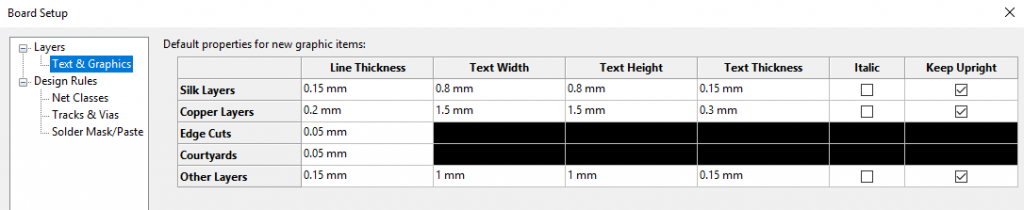
For example, one of the tutorials I learned with had silkscreen text with a 0.1mm size, but Elecrow don’t go under 0.15mm. It’s best to setup this first as a default value so you don’t need to adjust them. Also note that many sizes here are in mil and not in mm like in KiCad. Here is the basic setup for the board that KiCad will enforce while drawing and validating this project:
Board wiring
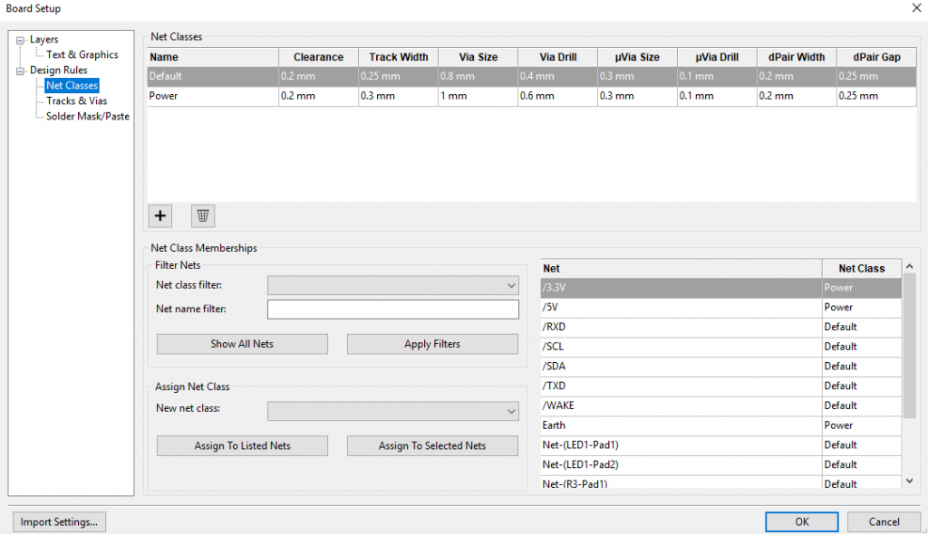
The number of copper layers is another option to setup before getting started drawing the traces. For a small DIY project such as this, two layers is pretty much standard so the default options are already fine. Generally, the copper layer on top (F.cu in KiCad) will have all the various tracks, and the bottom layer (B.cu in KiCad) will be filled with copper and used as the ground for all the components.
For projects with a lot more traces to place, additional layers can be added, but it’s best to avoid it at first. All the layers are sandwiched together during fabrication, so if you made a mistake in the inside layer you most likely won’t be able to fix it. If the layer is visible, you can sometimes cut a trace carefully and fix it with a small wire.
To place all the traces on the board, you will need to use the Route Track tool in KiCad while having the copper layer on which you wish to place the trace selected. KiCad will give you with thin lines indicating how the components are connected while you’re drawing.
For the layer that will serve as ground, the Add Filled Zone tool will allow you to draw a region that will be filled with coppers. All the through-hole pads that touch this zone will automatically be connected. At this point, if you have pads that are directly on the board, you’ll need to link them to that zone using the via tool.
Once it’s all done, the Design Rule Check tool can validate for you if all the traces are placed properly and all the design rules we specified earlier are still respected.
Silkscreen and other text layers
All the text on the silkscreen layers will be printed on the board when fabricating it. For a two layer board, you have a layer for the silkscreen in the front of the board (F.SilkS in KiCad) and another one for the back of the board (B.SilkS in KiCad). In this design, I only added text in front. You can use it to add the value and number of the various parts to help you build the PCB, or any other information about the project that’s useful for you. You can move and resize the existing text like you moved the components.
There is also text on the Fabrication (F.Fab in KiCad) layer, but those are only notes for you and will not be printed. If you want to print some of them, you can move the text to the silkscreen layer (or move text from the silkscreen layer to the fabrication layer if you don’t want to print some of them).
Ordering the PCB
When you’re ready to order the PCB, you’ll need to generate Gerber files to send to the fabrication house. There are many different files that will be generated for the project:
- The copper on the top and bottom of the board.
- The cutout of the board (mechanical layer).
- The holes to drill (plated and non-plated).
- The top and bottom solder mask.
- The top and bottom silkscreen.
In KiCad, choose the Plot option in Pcbnew to generate the files. In the popup, make sure to use the Plot option, and go to the Generate Drill Files… option to generate the drill file and the map file. Once they’re generated and in the same folder, just zip them all so you can send it over easily. Many fabrication houses have tools that will show you a preview of the content of the files; you can also test the content on http://gerblook.org/.
Once you have those files, there are many fabrications houses that will make a hobbyist project. Most have decent quality, but you’ll pay a lot more for a rush order. If you’re willing to wait, it’s more economical for them and for you since they fabricate large panels at once and will squeeze your board in some space they have left when then get a chance. Also, a local fabrication house will often be more expensive, but can ship the boards to you faster.
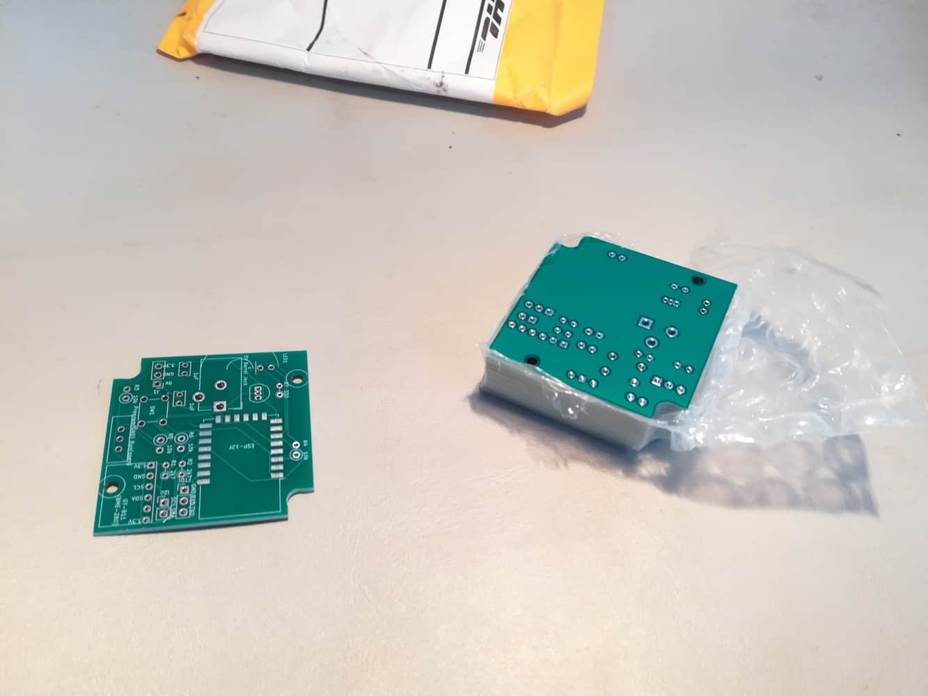
I was willing to wait for the fabrication and the shipping, so I went with Elecrow in China. Since it was my first board with them, the final price for 5 boards for 0.99$ USD, with 6$ USD of shipping to Canada. The standard price would have been 4.99$ USD for the boards without the special, which is still a very good price.
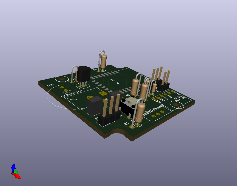
They kept me informed on the progression of my order with a picture of the completed boards as soon as they were done. The boards showed up at my door in less than 3 weeks, even with the slowest shipping option! Here they are, as I unwrapped them. I’m just waiting for the last parts to show up so I can solder them and check if I made any mistake in the design.
